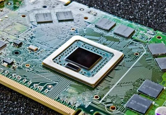
Modern electronic devices continue to become smaller while offering more advanced features and improved performance. This trend has increased the demand for printed circuit boards that can accommodate complex electrical connections within limited space. High-density interconnect technology has become an important solution for manufacturers developing compact electronic products that require dense component placement, precise routing, and reliable signal transmission.
HDI printed circuit boards use advanced design and manufacturing techniques to support finer traces, smaller vias, and higher connection density than many conventional PCB designs. These capabilities allow engineers to create sophisticated circuit layouts without significantly increasing board dimensions. For businesses developing advanced electronics, choosing an appropriate fabrication solution is essential for balancing circuit complexity, manufacturing quality, and overall project costs.
FastTurn PCBA provides PCB manufacturing and assembly solutions for businesses working on different electronic product requirements. Understanding rigid flex hdi pcb fabrication, its manufacturing processes, benefits, and design considerations can help engineers select suitable circuit technologies for their applications.
What Is HDI PCB Fabrication?
High-density interconnect PCB fabrication is the process of manufacturing circuit boards designed to support a high number of electrical connections within a relatively small area.
HDI boards typically use fine-line copper patterns, microvias, and compact component layouts to accommodate complex circuits. Depending on the design, they may also incorporate multiple conductive layers and advanced interconnection structures.
Traditional PCBs can become difficult to route when a design includes numerous components, dense connections, and limited board space. HDI technology addresses these challenges by providing additional routing flexibility and more efficient use of the available area.
Common characteristics of HDI PCBs include:
- Fine trace widths and spacing.
- Microvias for connecting circuit layers.
- High component density.
- Compact board dimensions.
- Multiple routing layers.
- Shorter electrical connection paths.
- Support for advanced electronic packaging.
- Flexible design options for complex circuits.
The specific capabilities of an HDI board depend on its layer stack-up, via structure, material selection, and manufacturing requirements.
Understanding Rigid-Flex HDI PCB Fabrication
Rigid-flex HDI hdi pcb fabrication combines high-density interconnect technology with rigid-flex circuit construction. This approach integrates dense circuit routing with flexible sections that connect rigid areas within a single board assembly.
The rigid sections provide stable mounting surfaces for electronic components, while the flexible sections allow the circuit to bend or fold according to the product’s mechanical design.
Combining these technologies can be useful when an electronic product requires both high connection density and a compact three-dimensional arrangement.
For example, a device may need a rigid section to support processors and other components while using a flexible section to connect displays, sensors, or separate internal modules.
Rigid-flex HDI designs can offer several advantages:
- Higher routing density within limited space.
- Reduced need for separate cables and connectors.
- Improved integration of electronic modules.
- Support for complex product shapes.
- Potential reductions in overall assembly size.
- Greater freedom when positioning circuit sections.
However, rigid-flex HDI designs are more complex than many conventional PCB structures. Engineers must carefully coordinate electrical routing, mechanical flexibility, layer transitions, and manufacturing tolerances.
Why Choose FastTurn PCBA for HDI PCB Manufacturing?
Selecting an appropriate manufacturing partner is important when developing high-density circuit boards. Complex PCB designs require careful attention to material properties, trace geometry, interlayer connections, and electrical performance.
FastTurn PCBA provides PCB manufacturing and assembly solutions for businesses developing electronic products with different technical requirements. Before beginning an HDI or rigid-flex HDI project, customers should confirm that the available manufacturing capabilities match their required board construction.
Support for Complex Circuit Designs
Advanced electronic products may require numerous connections within limited board dimensions.
HDI technology can help accommodate these requirements through fine-line routing and compact interconnections.
Engineers should provide complete design files and identify the required layer count, via structures, trace dimensions, and electrical specifications. This information helps establish the manufacturing requirements before production begins.
Custom PCB Requirements
Different applications have different electrical, mechanical, and environmental requirements.
A custom HDI board may require specialized materials, controlled impedance, particular copper thicknesses, or specific surface finishes.
Rigid-flex HDI projects may also require defined bend regions, flexible substrate materials, and carefully planned transitions between rigid and flexible areas.
Clearly documenting these requirements can help reduce misunderstandings and improve the design review process.
Fabrication and Assembly Planning
PCB fabrication and assembly requirements should be evaluated together, especially when the design includes fine-pitch components or compact layouts.
Component spacing, soldering requirements, thermal management, and inspection procedures can all affect the final manufacturing approach.
Planning these details early helps engineers identify possible production challenges before committing to a larger manufacturing run.
Key Benefits of HDI PCB Fabrication
HDI technology provides several advantages for electronic products that require dense routing and compact construction.
1. Higher Circuit Density
One of the primary benefits of HDI PCB fabrication is its ability to accommodate more electrical connections within a limited area.
Fine traces, smaller vias, and optimized layer arrangements allow engineers to route complex circuits without making the board unnecessarily large.
This capability is valuable for products containing processors, memory devices, communication modules, and other components with numerous connections.
2. Smaller and Lighter Electronic Products
Compact circuit layouts can help manufacturers reduce the size and weight of electronic assemblies.
By using board space more efficiently, engineers may be able to design smaller enclosures or integrate additional functionality into an existing product size.
When HDI technology is combined with rigid-flex construction, the circuit can also follow the physical arrangement of the product more closely.
The final size and weight savings depend on the complete design rather than HDI technology alone.
3. Improved Signal Performance
HDI designs can support shorter routing paths and more compact interconnections.
In suitable designs, shorter signal paths may help reduce parasitic effects and support high-speed signal transmission.
However, signal integrity depends on several factors, including trace geometry, dielectric properties, impedance control, reference planes, and routing strategy.
Engineers should evaluate these factors during design rather than assuming that a higher-density board automatically provides better electrical performance.
4. Greater Routing Flexibility
Microvias and additional routing options can help designers manage complex component connections.
This flexibility is particularly useful when a board contains fine-pitch components or dense ball grid array packages.
An optimized routing strategy can improve space utilization while maintaining the electrical characteristics required by the application.
5. Support for Advanced Components
Modern electronic components may contain a large number of connection points within a small package.
Conventional PCB routing can become challenging when connecting these components without increasing board size.
HDI structures can provide additional routing options that support dense component integration.
6. Potential Assembly Benefits
Compact circuit designs may reduce the number of separate boards, cables, and connectors required in some products.
When combined with an appropriate assembly strategy, this can simplify parts of the manufacturing process.
The actual benefits depend on the board design, component selection, production volume, and final product architecture.
HDI PCB Layer Structures and Via Technologies
The structure of an HDI PCB determines how its conductive layers connect and how effectively the design uses the available space.
Engineers must select an appropriate arrangement based on routing density, component requirements, electrical performance, and manufacturing capabilities.
Microvias
Microvias are small-diameter interconnections used to connect conductive layers in HDI circuit boards.
They can provide routing options that are difficult to achieve with conventional through-hole vias in dense layouts.
Microvias may connect adjacent layers or form part of more complex interconnection structures.
Their dimensions, aspect ratios, and reliability requirements must be compatible with the selected manufacturing process.
Blind Vias
Blind vias connect an outer conductive layer to one or more internal layers without extending through the entire board.
This construction can help preserve routing space on other layers.
Blind vias are useful in designs where component density and limited board dimensions create significant routing challenges.
Buried Vias
Buried vias connect internal conductive layers without opening onto the external surfaces of the PCB.
They can provide additional routing options while preserving surface area for component placement and external connections.
Their implementation depends on the layer stack-up and manufacturing process.
Stacked and Staggered Microvias
HDI boards may use stacked or staggered microvias to connect multiple conductive layers.
Stacked microvias are positioned vertically over one another, while staggered microvias use offset positions.
Each approach has different manufacturing and reliability considerations.
The correct choice depends on the board structure, electrical requirements, fabrication capabilities, and expected operating conditions.
Sequential Lamination
Some HDI structures require sequential lamination, in which layers are built and bonded through multiple manufacturing stages.
This process supports complex layer arrangements and microvia structures.
Because additional processing stages can increase manufacturing complexity, the stack-up should be designed carefully to meet the application’s requirements without unnecessary complications.
The HDI PCB Fabrication Process
HDI PCB fabrication involves several carefully controlled stages. The exact process depends on the board’s layer count, via arrangement, material selection, and manufacturing specifications.
1. Design Review and File Preparation
The process begins with reviewing the PCB layout and preparing the manufacturing documentation.
Engineers should verify that the design files match the intended board revision and contain all necessary technical information.
Important details include:
- PCB layout and copper layer files.
- Drill files.
- Layer stack-up specifications.
- Trace widths and spacing.
- Microvia dimensions.
- Blind and buried via requirements.
- Controlled impedance specifications.
- Material and copper thickness requirements.
- Surface finish requirements.
- Electrical testing expectations.
For rigid-flex HDI boards, the documentation should also identify rigid and flexible regions, bend locations, and the materials required for each section.
2. Material Selection
Material selection affects the electrical, thermal, and mechanical behavior of the finished board.
Standard FR-4 materials are suitable for many applications, while some high-speed or high-frequency designs may require specialized laminates.
Rigid-flex HDI boards may use different materials in their rigid and flexible sections.
Engineers should consider dielectric properties, thermal expansion, operating temperature, signal speed, and mechanical flexibility when choosing materials.
3. Inner-Layer Circuit Patterning
For multilayer boards, the inner copper layers are patterned according to the approved circuit design.
This process creates the traces, pads, and electrical features required for routing signals and distributing power.
Fine-line designs require accurate pattern formation because small variations can affect electrical performance and manufacturing yield.
4. Lamination
The conductive and insulating layers are combined to form the required PCB structure.
Depending on the HDI design, fabrication may include multiple lamination stages.
Careful process control helps maintain layer alignment and supports reliable interconnections between conductive layers.
5. Laser Drilling and Microvia Formation
Laser drilling is commonly used to create microvias in HDI PCBs.
These small openings provide connections between selected conductive layers.
The drilling process must be appropriate for the board materials and the intended via dimensions.
Accurate microvia formation is essential for creating reliable interlayer connections.
6. Via Metallization and Copper Plating
After drilling and preparation, the via walls are processed to establish electrical connections between the relevant layers.
Copper plating provides the conductive structure required for interlayer connections.
The process must meet the design’s electrical and manufacturing requirements, particularly in dense multilayer constructions.
7. Outer-Layer Patterning
The external copper layers are patterned to create the required traces, pads, and connection points.
Fine trace spacing and small pad dimensions require precise manufacturing controls.
The finished patterns must match the approved design files and remain compatible with the intended assembly process.
8. Solder Mask and Surface Finishing
A solder mask may be applied to protect exposed copper areas and help prevent unintended solder connections during assembly.
The selected surface finish protects exposed pads and supports solderability or other electrical contact requirements.
Common finishes include electroless nickel immersion gold and other options selected according to the design and manufacturing needs.
9. Electrical Testing and Inspection
The finished PCB should undergo appropriate inspection and testing before acceptance.
Depending on the project, this may include:
- Visual inspection.
- Dimensional verification.
- Electrical continuity testing.
- Insulation testing.
- Microvia and interconnection inspection.
- Layer registration checks.
- Impedance testing where required.
- Surface finish inspection.
- Functional testing after assembly.
For rigid-flex HDI boards, additional checks may be needed to verify flexible-section dimensions, bend-region construction, and other mechanical requirements.
Important Design Considerations for Rigid-Flex HDI PCB Fabrication
Combining HDI technology with rigid-flex construction requires careful planning because electrical routing and mechanical flexibility must work together.
Trace Width and Spacing
HDI boards often use fine traces and narrow spacing to accommodate dense routing.
However, smaller dimensions require tighter manufacturing tolerances and may increase fabrication complexity.
Designers should choose trace widths and spacing based on current requirements, voltage constraints, signal performance, and the manufacturer’s capabilities.
Microvia Reliability
Microvias are important elements of many HDI designs, but their reliability depends on geometry, material properties, plating quality, and thermal conditions.
Stacked microvias can introduce additional manufacturing considerations.
The selected via structure should be appropriate for the board’s layer arrangement and expected operating environment.
Flexible Region Design
In rigid-flex HDI boards, flexible regions must be designed according to their intended movement.
Copper traces should be routed with mechanical stress in mind, and sensitive interconnections should be positioned carefully.
Designers should distinguish between static bends used during installation and dynamic bends that occur repeatedly during operation.
Bend Radius
An excessively tight bend can damage copper traces, insulation, or bonding materials.
The appropriate bend radius depends on the flexible stack-up, total thickness, copper construction, and expected bending cycles.
Material-specific recommendations and manufacturing guidance should be followed when defining bend locations.
Thermal Management
Dense electronic designs can concentrate heat within small areas.
Thermal management should be considered when selecting materials, positioning components, defining copper planes, and planning the overall circuit structure.
Rigid-flex designs require particular attention because the thermal behavior of flexible and rigid sections may differ.
Signal Integrity and Impedance Control
High-speed circuits may require controlled impedance, carefully designed reference planes, and optimized routing.
Transitions between layers and between rigid and flexible regions can influence electrical performance.
Engineers should evaluate the complete signal path rather than focusing only on individual trace dimensions.
Design for Manufacturability
Design for manufacturability involves developing the circuit so it can be produced consistently within the available manufacturing capabilities.
For HDI boards, this includes reviewing via dimensions, aspect ratios, trace spacing, layer registration, and stack-up complexity.
For rigid-flex designs, the review should also consider flexible materials, bend regions, and transitions between rigid and flexible sections.
A design review before fabrication can help identify potential problems and avoid unnecessary redesigns.
Applications of HDI PCB Fabrication
HDI PCBs support electronic products that require compact layouts, dense connections, and reliable electrical performance.
Consumer Electronics
Smartphones, tablets, digital cameras, wearable devices, and portable electronics often require dense circuit layouts.
HDI technology helps accommodate complex components within limited board dimensions.
Rigid-flex HDI structures can also connect different sections of a compact device while reducing the need for separate cables.
Medical Equipment
Medical electronics may require compact circuits for diagnostic equipment, monitoring devices, imaging systems, and specialized instruments.
HDI technology can support dense component integration in products with limited internal space.
Medical applications may require additional controls related to electrical safety, reliability, material compatibility, and applicable regulatory standards.
Automotive Electronics
Modern vehicles use complex electronic systems for sensing, control, communication, navigation, and driver assistance.
HDI PCBs can help integrate these functions within compact electronic modules.
Rigid-flex HDI designs may be appropriate for selected assemblies that require compact layouts and flexible interconnections.
Automotive applications should be evaluated for temperature changes, vibration, moisture exposure, and other environmental conditions.
Telecommunications
Telecommunications equipment often requires high-speed signal routing and dense component integration.
HDI designs can support compact networking devices, communication modules, and other electronic systems.
Material selection, impedance control, and signal integrity are particularly important in applications involving high-speed data transmission.
Aerospace and Defense
Aerospace and defense systems may impose strict requirements for size, weight, electrical performance, and reliability.
HDI and rigid-flex HDI boards can support selected applications where compact construction is beneficial.
Depending on the project, specialized materials, qualification procedures, traceability, and environmental testing may be necessary.
Industrial Automation
Industrial controllers, sensors, robotics, and monitoring equipment may require complex circuit layouts within compact housings.
HDI boards can help accommodate advanced processing and communication functions.
The final design should reflect the operating temperature, electrical load, vibration conditions, and expected service life.
HDI PCB vs. Conventional PCB Fabrication
HDI and conventional PCB technologies serve different design needs. The appropriate choice depends on circuit complexity, available space, electrical performance, and manufacturing budget.
| Feature | HDI PCB | Conventional PCB |
| Circuit Density | Supports very dense routing | Suitable for standard routing requirements |
| Trace Dimensions | Can support finer traces and spacing | Often uses larger trace dimensions |
| Via Technology | May use microvias, blind vias, and buried vias | Commonly uses through-hole vias |
| Component Integration | Suitable for dense, fine-pitch components | Suitable for many standard components |
| Manufacturing Complexity | Generally higher for advanced designs | Often simpler |
| Initial Cost | Can be higher due to specialized processing | Often more economical for straightforward layouts |
| Typical Applications | Compact, advanced electronics | General electronic products and less dense designs |
Not every product requires HDI technology. A conventional PCB may be more economical and easier to manufacture when the design has sufficient space and relatively straightforward routing requirements.
Engineers should evaluate the benefits of higher circuit density against the additional manufacturing complexity and cost.
How to Choose the Right HDI PCB Manufacturing Partner
Selecting a suitable manufacturing partner is an important decision for businesses developing advanced electronic products.
Evaluate Technical Capabilities
Confirm that the manufacturer can support the required layer count, microvia dimensions, trace widths, spacing, materials, and board thickness.
For rigid-flex HDI projects, verify the availability of the required rigid-flex construction and flexible material options.
Review Quality Control Procedures
Ask about electrical testing, visual inspection, via quality checks, and dimensional verification.
For demanding applications, determine whether the manufacturer can provide the documentation and testing required by the project.
Consider Engineering Support
Manufacturing expertise can help identify problems related to stack-up selection, via geometry, signal routing, and bend-region placement.
A thorough design review may also identify opportunities to simplify the design without compromising performance.
Assess Production Requirements
Consider the expected prototype quantity, future production volume, delivery schedule, and potential design revisions.
The manufacturing approach should support the project’s current needs while allowing for future development.
Compare Total Project Value
Manufacturing cost is important, but it should be considered alongside product quality, engineering support, production consistency, and testing capabilities.
A suitable manufacturing partner can help businesses balance technical requirements with practical budget constraints.
How FastTurn PCBA Supports High-Density Circuit Board Development
FastTurn PCBA provides PCB manufacturing and assembly solutions for businesses developing electronic products with different levels of circuit complexity.
For HDI and rigid-flex HDI projects, customers should provide complete design files and specify the required stack-up, via structures, trace dimensions, materials, copper thickness, surface finish, and electrical testing requirements.
Where the design includes flexible regions, the documentation should also identify bend locations, minimum bend radius, and whether the circuit will experience repeated movement.
Businesses should confirm the availability of specialized manufacturing processes and assembly capabilities before finalizing their production plans.
Clear technical documentation helps establish manufacturing expectations and supports a more organized development process.
By evaluating the circuit structure, manufacturing requirements, and intended operating environment early, businesses can make better-informed decisions when preparing advanced FastTurn PCBA designs.
Conclusion
HDI PCB fabrication enables manufacturers to develop high-density circuit boards that accommodate complex electrical connections within limited space. Through fine-line routing, microvias, and advanced layer arrangements, HDI technology supports compact electronic products that require efficient component integration and carefully controlled signal performance.
Combining HDI technology with rigid-flex construction can provide additional design flexibility for applications that require both dense circuit routing and flexible interconnections. However, successful rigid flex hdi pcb fabrication depends on careful material selection, stack-up planning, via design, bend-radius control, signal integrity, and manufacturing quality.
FastTurn PCBA provides PCB manufacturing and assembly solutions for businesses developing advanced electronic products. By defining technical requirements clearly and evaluating manufacturing capabilities before production, engineers can better prepare their designs for fabrication, assembly, and testing.
Whether the application involves consumer electronics, medical equipment, automotive systems, telecommunications, or industrial technology, selecting an appropriate PCB structure can help support compact designs, reliable electrical connections, and efficient product development.
